Why we’re ditching the old ovens for IR curing
For a long time, semiconductor fabrication relied on those massive convection ovens. But honestly? They’re becoming relics. We’re moving toward infrared (IR) curing now, mostly because it actually hits those “green” and lead-free targets that everyone is chasing these days. Instead of just blowing hot air around, IR uses electromagnetic radiation. It goes straight for the wafer surface. No middleman.
Getting the heat where it actually belongs
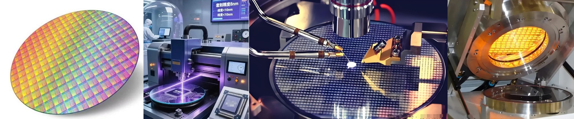
Think about how a convection oven works. You heat the air, and then the air heats the wafer. It’s a waste of power. IR is different. It bypasses all that. The photons dive right into the photoresist or solvent layer and trigger a reaction immediately. The best part? We can stop using those nasty toxic catalysts and lead-based stabilizers that used to be the norm. We usually stick with short-wave IR for this. It packs the most punch. Because the heat hits so hard and fast, the wafer spends way less time in the heating zone. Less time under the lamp means lower power bills. Simple as that.
The tricky part (The engineering)
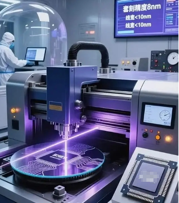
Now, you can’t just rip out an old heater and plug in an IR lamp. It doesn’t work like that. These lamps put out an incredible amount of heat. If your chassis isn’t built for it, you’re going to fry your sensors and melt your electronics. You absolutely need a solid cooling manifold to keep the rest of the hardware from cooking. And then there’s the “over-curing” headache. If your conveyor belt is moving too slowly, you’ll warp those thin wafers. It’s a balancing act. You have to tweak the wattage and the line speed until the thermal profile is just right.
Doing right by the planet
The nice thing about IR is that it doesn’t vent combustion gases. there are no VOCs coming off the heating element. When you cut drying time from minutes down to seconds, your carbon footprint shrinks. It’s a great way to replace those old, leaky thermal tunnels that suck up power and turn your cleanroom into a sauna.